Bose 1600-VI Service Manual
Browse online or download Service Manual for Audio amplifiers Bose 1600-VI. Bose 1600-VI Service manual [en] User Manual
- Page / 60
- Table of contents
- BOOKMARKS
- Stereo Power Amplifiers 1
- CONTENTS 2
- SAFETY INFORMATION 4
- DEVICE HANDLING 4
- 1800VI SPECIFICATIONS 5
- 1600VI SPECIFICATIONS 7
- VI and 1800VI Block Diagram 9
- THEORY OF OPERATION 10
- Figure 5. 240V 21
- Configuration 21
- TEST PROCEDURES 31
- PART LIST NOTES 34
- PART LISTS AND EXPLODED VIEWS 34
- MAIN PART LIST 35
- Attaches 38
- 240V Configuration 39
- ELECTRICAL PART LIST 41
- PACKING LIST 55
- WIRING DIAGRAMS 56
- IC PINOUT DIAGRAMS 58
- Bose Corporation 60
- The Mountain 60
Summary of Contents
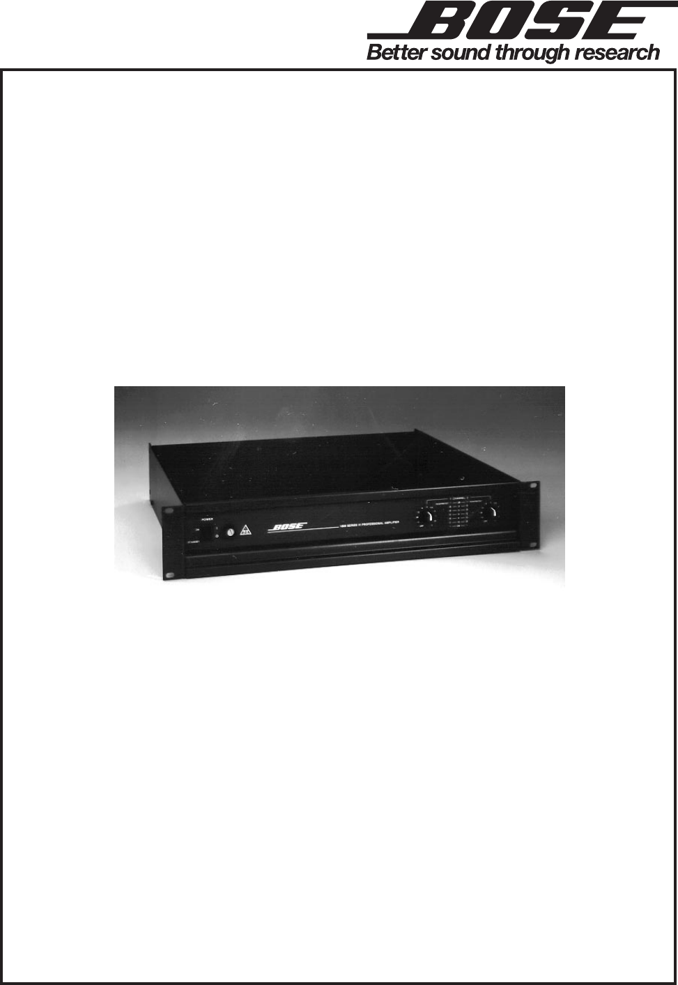
®®©1998 Bose CorporationModel 1600VI and 1800VI ProfessionalStereo Power AmplifiersPart Number 199747 Rev. 00Service Manual
10THEORY OF OPERATION1. GeneralThe Bose® Model 1600VI and 1800VI Professional Stereo Power Amplifiers are two-channel,installed/portable amplifiers ma
11THEORY OF OPERATION2.1 Input ModuleNote: Some amplifiers will be equipped with the Bose® ACM-1 Amplifier Control Module inplace of the Bose Input Mo
12THEORY OF OPERATIONWhen SW1 is set to the NORMAL mode, CH1 and CH2 operate independently. In this mode alogic high is applied to the control pins of
13THEORY OF OPERATION2.3 Output RelaysNote: Refer to the Output PCB schematic for the following.Relay K100 is used to connect the output signal to the
14THEORY OF OPERATIOND2 and D3 on the Regulator Board provide overvoltage protection to U4. U4B-14 is a full-waverectifier that outputs positive pulse
15THEORY OF OPERATIONThe -15Vdc supplied to U5A-4 is backed up with a voltage divider off the -106Vdc supply (R26/R27). Without this, if the -15Vdc su
16THEORY OF OPERATIONThe output signal is sensed at the speaker output via the I/O Board (J2-3 Output Board to J6-3I/O Board to J3-6 I/O Board to J1-6
17THEORY OF OPERATION3.2 Clipping Eliminator CircuitThis circuit is controlled by the LED/LDR opto-isolator U3, located on the I/O Board. The LEDporti
18THEORY OF OPERATION4.0 Operating ModesThe Bose® 1600VI and 1800VI amplifiers are capable of being configured to operate in severaldifferent modes in
19DISASSEMBLY/ASSEMBLY PROCEDURESNote: It's advisable to mark or note wiringconfiguration before any disassemblybegins. For more information refe
2CONTENTSSafety Information...
20Figure 4. Rear View - Attaching Hardware3AC1800 W50-60Hz100VCONSULTOWNERS MANUAL1800 SERIES V PROFESSIONAL AMPLIFIERLICENSED UNDER U.S. PAT. NO. 4,4
21Figure 6. 1600VI and 1800VI Amplifier AssemblyAAR101R1023297620Qty 2Qty 6Power SupplyBoardQty 2844Qty 285Display Board45Qty 220Qty 21950Regulator Bo
22I/O BoardPart of92164317234T1J12824B1Qty 211Qty 4262712333432678910112153410Qty 21112FL1E11214Qty 4F1Qty 240513741Qty 43742Qty 2P131LOADLINEQty 225O
23DISASSEMBLY/ASSEMBLY PROCEDURES6.2 Carefully line up the holes of theregulator board with the nylon standoffsmounted on the power supply board.Snap
24DISASSEMBLY/ASSEMBLY PROCEDURESNote: Refer to Figures 5, 6 and 7 for thefollowing procedures.9. Line Filter Removal9.1 Remove the cover (1) usingpro
2514.5 Connect the amplifier and powersupply board (7) cables to the output board(16) WL1, WL2, WL100, WL101, WL200and WL201 terminals. Refer to Wirin
26DISASSEMBLY/ASSEMBLY PROCEDURES16.4 Connect the output board black wiresto the binding posts (items 24 or 25) bytightening four nuts with a wrench.
27DISASSEMBLY/ASSEMBLY PROCEDURESFigure 9. Heatsink Bridge17.3 Disconnect the amplifier board (15)ribbon cable from the power supply (7)J2 connector.1
28DISASSEMBLY/ASSEMBLY PROCEDURES18. Power Supply Board Replacement18.1 Attach the power supply board (7) tothe heatsink (18) by tightening four screw
29DISASSEMBLY/ASSEMBLY PROCEDURESNote: Refer to Figure 6 for the followingprocedures.21. I/O Board Removal21.1 Use Procedure 15, Steps 15.1-15.12to re
3PROPRIETARY INFORMATIONTHIS DOCUMENT CONTAINS PROPRIETARY INFORMATION OFBOSE® CORPORATION WHICH IS BEING FURNISHED ONLY FORTHE PURPOSE OF SERVICING
30DISASSEMBLY/ASSEMBLY PROCEDURESthe opening in the rear of the amplifier forthe ACM-1 module. Pin 1 is to the right.This corresponds to the red strip
31TEST PROCEDURESFigure 11. EQ Card PlacementTest Setup Parameters:1. In order to test these amplifiers at fullpower, you will need at least one 4Ω, 5
32TEST PROCEDURES3. Distortion Level3.1 Apply a 1.5 Vrms, 1 kHz signal for lowsensitivity units, or a 775 mVrms, 1 kHzsignal for high sensitivity unit
33TEST PROCEDURES8. Potentiometer Tracking Test8.1 Apply a 16 mVrms, 1 kHz signal to bothchannels of the amplifier under test.8.2 With both gain pots
34PART LIST NOTES1. This part is not normally available from Customer Service. Approval from the Field Service Manager is required before ordering.
35MAIN PART LISTItemNumberDescription Part Number Qty. Note1 Cover, PC, Gray 182740 12Chassis, 1800VI, DOM182739 1 5, 6, 9 1800VI, ECE1
36MAIN PART LISTItemNumberDescription Part Number Qty. Note28 Screw, MA, FHP, 6-32 x 1-1/4, blk, upper fanshield182718 429 Screw, STP, PHP, 4 x 1/2, A
37MAIN PART LISTItemNumberDescription Part Number Qty. Note- Standoff, .280d x .625l, Locking Nylon, betweenpwr supply and reg.199751 3- Standoff, PEM
38Figure 15. Cross Section ViewAIR FLOW51Qty 2385214Qty 4133512Qty 221Qty 4182922Qty 23Qty 43Qty 430Attachesclamp
39Figure 16. 1600VI and 1800VI Amplifier Top ViewLINELOAD240V Line Filter539240V ConfigurationR101R1023297620Qty 2Qty 6Qty 2844Qty 28545Qty 220Qty 219
4SAFETY INFORMATIONELECTROSTATIC DISCHARGE SENSITIVE (ESDS)DEVICE HANDLINGThis unit contains ESDS devices. We recommend the following precautions when
40I/O BoardPart of92164317234T1J1A32824B1Qty 211Qty 4262712333432678910112153410Qty 21112FL1E11214Qty 4F1Qty 240513741Qty 43742Qty 2P131LOADLINEQty 22
41ELECTRICAL PART LISTAmplifier PCB AssemblyResistorsCapacitorsReference Designator Description Part Number NoteC101, 201 30pF, Ceramic Disc, 10%,1000
42ELECTRICAL PART LISTCapacitorsReference Designator Description Part Number NoteC106, 206 22pF, Ceramic Disc, 10%,1000V182776C109, 209 4.7uF, AE, AXL
43ELECTRICAL PART LISTPower Supply PCB AssemblyResistorsCapacitorsReference Designator Description Part Number NoteC1, 2 .10uF, MP, 250VAC,UL/CSA18284
44ELECTRICAL PART LISTCapacitorsReference Designator Description Part Number NoteC12, 18, 21, 28, 32, 35, 42, 43 .0018uF, PE, Radial, 10%,100V182840C1
45Integrated CircuitsReference Designator Description Part Number NoteU1 Opto-Triac Driver,MOC3052182880U2, 3 Dual Volt Comparators,LM393182879Miscell
46CapacitorsReference Designator Description Part Number NoteC2, 23 1uF, AE, Radial, 20%,100V182898C3, 29 .18uF, MPE, 5%, 50V 182893C4, 5 270pF, CRML,
47ELECTRICAL PART LISTDiodesReference Designator Description Part Number NoteD1, 2, 6, 7, 8, 9, 12, 13, 14, 15, 16, 17,18, 20, 21, 22, 23, 24, 27, 29,
48Output PCB AssemblyELECTRICAL PART LISTResistorsReference Designator Description Part Number NoteR1 130Ω, Metal Oxide Film,3W, 5%182932R2 910Ω, MF,
49ELECTRICAL PART LISTIntegrated CircuitsReference Designator Description Part Number NoteU1 Dual Volt Comparators,LM393182879MiscellaneousReference D
5Size: 3.5"H (2U) x 19"W x 13.25"D89mm x 483mm x 337mmWeight: Net: 33 lbs. (15 kg)Shipping weight: 39 lbs. (17.7 kg)Display: 7 LED indi
50ELECTRICAL PART LISTRegulator PCB AssemblyNote: The Regulator PCB Assembly is not used in the 1600VI AmplifierResistorsReference Designator Descript
51ELECTRICAL PART LISTDiodesReference Designator Description Part Number NoteD2, 3 Zener, 1N4736A, 6.8V 182961D4, 5, 7, 8, 9 1N4148 182868D6 Zener, 1N
52CapacitorsReference Designator Description Part Number NoteC1, 2 1uF, AE, AXL, 20%, 50V 182973C3, 4, 5, 6 .01uF, CRML, Radial, +80-20, 100V182780Dio
53ELECTRICAL PART LISTInput Module PCB AssemblyResistorsReference Designator Description Part Number NoteR52, 53, 54, 55, 60, 62 332k, MF, 1/4W, 1% 18
54ELECTRICAL PART LISTTransistorsReference Designator Description Part Number NoteQ1 NPN, MPSA06, TO-92 182874Q2, 3 PNP, MPSA56, TO-92 182875Integrate
55PACKING LIST1600VI and 1800VI Amplifiers (see Figure 18)(4)13425IFigure 18. 1600VI and 1800VI Amplifiers Packing DiagramItemNumberDescription Part N
56SWITCHW24INPUTMODULEBOARDI/OBOARDDISPLAYBOARDAMPLIFIERBOARDP2P3-++-FANW19W4W3W10W9E200E100J201J101J1J1J6J3W18W13J2J200W12J100W11J3W8J1J2W1W2SWFUSEW3
57WL1WL2WL3E1E2E3SWITCHPCBW24W22E16WL6WL7W60W3E17W5W1W2SWITCHFUSEF1REDWHTBLU/BLKJ1J1REGULATORBOARD(Not used in1600VI Amp)POWERSUPPLYBOARDTIPRINGWL4WL5
58Bose® Part Number 182821, TL072Bose Part Number 182878, IRFZ44Bose Part Number 182880, MOC3052Bose Part Number 182879, LM393Bose Part Number 182963,
59IC PINOUT DIAGRAMSBose Part Number 182965, CNY17-2Bose® Part Number 182964, MC3405PBose Part Number 199766, VTL5C4Bose Part Number 183005, SSM214112
6Input Overload: +18 dBuIM Distortion: < 0.1%THD: @ 0.775 V Sensitivity, < 0.2%@ 1.5 V Sensitivity, < 0.1%Signal-to-Noise Ratio: > 100 dB,
P/N: 199747 Rev. 00 12/98 FOR TECHNICAL ASSISTANCE OR PART ORDERS, CALL 1-800-367-4008Bose CorporationThe MountainFramingham, Massachusetts USA 01701®
7Size: 3.5"H (2U) x 19"W x 13.25"D89mm x 483mm x 337mmWeight: Net: 30 lbs. (13.6 kg)Shipping weight: 36 lbs. (16.3 kg)Display: 7 LED in
8Input Overload: +18 dBuIM Distortion: < 0.1%THD: @ 0.775 V Sensitivity, < 0.2%@ 1.5 V Sensitivity, < 0.1%Signal-to-Noise Ratio: > 100 dB,
9AmplifierCH 1CH 2CH 2CH 1CH 1 CH 2OUT OUTCH 1OUTCH 2OUTOutputRelaysFan DriveCommutationControl(Class H)Power SuppliesOn/OffStandbySequenceFuse(230V)O
More documents for Audio amplifiers Bose 1600-VI


Related products and manuals for Audio amplifiers Bose 1600-VI
 (2 pages)
 (11 pages) (8 pages)
© 2020, manymanuals.com. All rights reserved. | 1.473 s |
 Manymanuals.com
 Manymanuals.de
 Manymanuals.fr
 Manymanuals.it
 Manymanuals.pl
 Manymanuals.cz
 Manymanuals.es
 Manymanuals-pt.com
Comments to this Manuals